

离岸价格
获取最新报价0.5 ~ 50 USD / Piece ( Negotiable )
|10 Piece Minimum Order
国家:
China
型号:
INVMC003
离岸价格:
0.5 ~ 50 USD / Piece ( Negotiable ) 获取最新报价
位置:
ZHANGZHOU
最小订单价格:
0.5 per Piece
最小订单:
10 Piece
包装细节:
Export Carton / Wooden Box/ Pallet
交货时间:
30 days after payment
供应能力:
10000 Piece per Month
付款方式:
T/T, Western Union
產品組 :
联系人 Wilson
Xiamen, Fujian
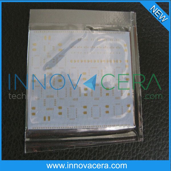
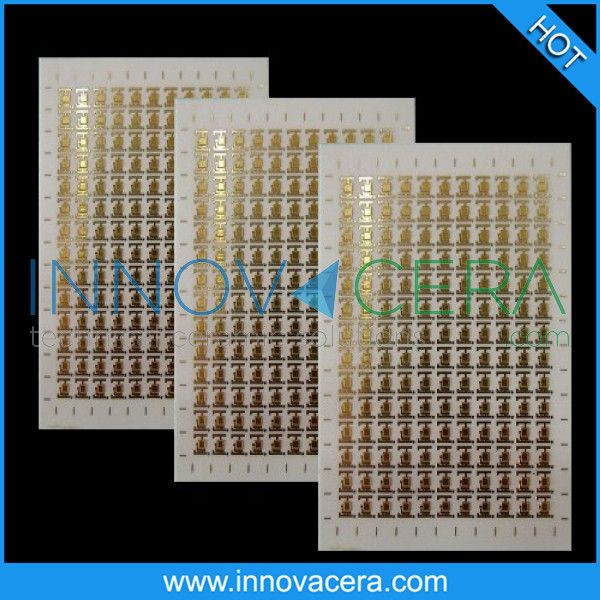
Alumina Thin film metallized ceramic substrate
high quality al2o3 metallized ceramic substrate
Electrical insulating alumina Al2O3 ceramic substrate plate
thick film alumina ceramic substrate
metalized ceramic substrate
Ceramic substrate pcb plate
As an expert manufacturer of ceramics, Innovacera has a complete range of advanced technical ceramics for a wide variety of applications.
Innovacera provides electronic ceramic substrate including Al2O3 (Alumina substrate)
and
AlN (Aluminum Nitride substrate). These ceramic substrate have good mechanical strength and abrasion resistance, high thermal conductivity , very stable in high temperature and corrosive chemical and excellent electrical insulation.
Alumina ceramic is kind of structural ceramics, with insulation resistance, voltage resistance, high strength, good thermal conductivity, dielectric loss, stable electrical performance characteristics. Used in electronic ceramic substrates, ceramic electrical insulation, vacuum devices, devices porcelain, spark plugs and other products. We can make the part by hot injection pressing, dry pressing, isostatic pressing and extrusion productive technology etc.
Overview of Main Physical Properties:
1.Good electrical insulation
2.High mechanical strength
3.Excellent wear resistance
4.Excellent corrosion resistance
5.Low dielectric constant
Overview of Main Applications:
1. High Power LED ceramic substrate
2. Microwave (Wireless Communication & Radar)
3. Semiconductor Process Equipment
4. Solar Cell
5. Hybrid Electric Vehicles
6. Flip chip/eutectic substrate
7. Sensor ceramic substrate
Different Kinds of Substrates:
We can provide various kind of metallizations as below:
1.Thin Film Ceramic Substrate
This product is widely used in circuit substrates for optical storage, optical communication, RF application, LED and various other uses.
2.Thick Film Ceramic Substrate
This product is widely used in circuit substrates for optical storage, optical communication, RF application, LED and various other uses.
|
Difference between thin & thick film patterns |
||
|
Thin Film Patterns |
Thick Film Patterns |
|
|
Better pattern accuracyof +/*1% |
Normal Pattern accuracyof +/**0% |
|
|
Higher surface roughness of <0.3um |
Poor surface roughness of 1~3um |
|
|
Goodsurface adhesion in both Al2O3 and AlN |
Good surface adhesion in Al2O3 but poor adhesion in AlN |
|
|
Good alignment accuracy |
Poor alignment accuracy |
|
|
Higher materialstability (Cu layer) |
Normal materialstability (Ag and glass mixture) |
|
We are ISO certified:
ISO***1:***8 ISO****1:***4 OHSAS****1:***9
Superior quality of products with reliance is our prime consideration.
Feel free to contact us if you need any other assistance about our products.
We care and provide what you want!
| 国家: | China |
| 型号: | INVMC003 |
| 离岸价格: | 0.5 ~ 50 / Piece ( Negotiable ) 获取最新报价 |
| 位置: | ZHANGZHOU |
| 最小订单价格: | 0.5 per Piece |
| 最小订单: | 10 Piece |
| 包装细节: | Export Carton / Wooden Box/ Pallet |
| 交货时间: | 30 days after payment |
| 供应能力: | 10000 Piece per Month |
| 付款方式: | T/T, Western Union |
| 產品組 : | Metallized Ceramics |