联系人 Ms. Helen
4th Floor, Building A, 2nd West side, West zheng 2nd Road, Shajiao Community, Dongguan, Guangdong
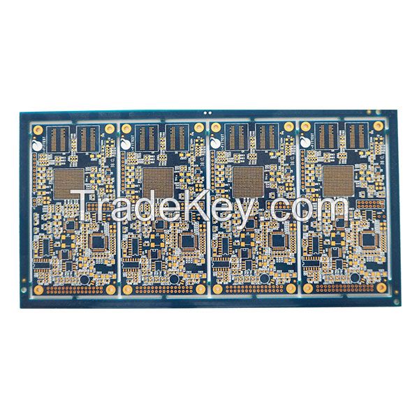
Material type: FR4
Layer count: 4
Min trace width/space: 4 mil
Min hole size: 0.*0mm
Finished board thickness: 1.*0mm
Finished copper thickness: *5um
Finish: ENIG
Solder mask color: blue
Lead time: *5 days
Buired hole:
The through hole between the inner layers, after pressing, cannot be seen, so it does not need to occupy the outer area, the upper and lower sides of the hole are in the inner layer of the board, in other words, buried in the board
Blinded hole:
It is used for the connection between the surface layer and one or more inner layers. One side of the hole is on one side of the board, and then the hole is connected to the inside of the board.
The advantage of the blinded and buried hole board:
In non-perforating hole technology, the application of blind hole and buried hole can greatly reduce the size of PCB, reduce the number of layers, improve the electromagnetic compatibility, increase the characteristics of electronic products, reduce the cost, and also make the design work more simple and fast. In traditional PCB design and processing, through-hole can cause many problems. Firstly, they occupy a large amount of effective space. Secondly, a large number of through-holes in a dense area also cause great obstacles to the wiring of the inner layer of multi-layer PCB. These through-holes occupy the space needed for wiring, and they densely pass through the surface of the power supply and ground wire layer, which will destroy the impedance characteristics of the power supply ground wire layer and cause the failure of the power supply ground wire layer. And conventional mechanical drilling will be *0 times as much as the use of non-perforating hole technology.
| 国家: | China |
| 型号: | - |
| 离岸价格: | ( Negotiable ) 获取最新报价 |
| 位置: | - |
| 最小订单价格: | - |
| 最小订单: | 1 Piece |
| 包装细节: | - |
| 交货时间: | - |
| 供应能力: | - |
| 付款方式: | - |
| 產品組 : | - |


")


